English
 中文
中文

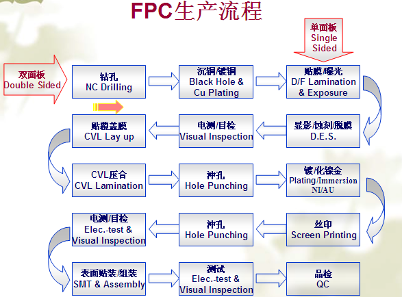
Based on the difficulty of processing by the subtractive method or the difficulty in maintaining a high-yield fine circuit, it is considered that the semi-additive method is an effective method, and various schemes of the semi-additive method have been proposed. Example of microcircuit processing by semi-additive method. The semi-additive process takes the polyimide film as the starting material, and firstly casts (coats) the liquid polyimide resin on a suitable carrier to form the polyimide film.
Next, a crystal-planting layer is formed on the polyimide base film by sputtering, and a resist pattern of the reverse pattern of the circuit is formed on the crystal-planting layer by photolithography, which is called a plating-resistant layer. Conductor circuits are formed by electroplating on the blank portions. Then, the resist layer and the unnecessary seeding layer are removed to form the first layer of circuits. Coat the photosensitive polyimide resin on the first layer of circuit, form holes, protective layer or insulating layer for the second layer of circuit layer by photolithography, and then sputter on it to form a crystal planting layer as the first The base conductive layer of the two-layer circuit. By repeating the above process, a multilayer circuit can be formed.
According to Xinyingtongda Technology, this semi-additive method can process ultra-fine circuits with a pitch of 5um and a via hole of 10um. The key to using the semi-additive method to fabricate ultrafine circuits lies in the properties of the photosensitive polyimide resin used as the insulating layer.